( Version Française, ici )
(2
clicks on every photos can give you a full view of schematics)
Presentation
The
terminal which I will describe, is an alpha numeric display built in
1969,
which uses TV delay lines as memory elements. It was
originally studied
in the Netherlands (Philips), and reached french engineering
under the brand name RTC
(French subsidiary of Philips Components).
In 1969, there was not yet integrated circuits offers in memory. It was still using the memory of ferrite cores, or other technology, such as acoustic mercury delay lines, or memories using switching capacitors capabilities.
This terminal display uses a standard television set, in a non-interlaced (312 lines, 50 frames per second: european standard). In reality the tube of this terminal had a long decay phosphorus, and a anti glare treatment.
The television industry used for decoding of the color, new delay lines of 64 uS (multi reflex). [You know, the sequence of our French SECAM Color: Red / Blue / Red / B / R / B ...]. The bandwidth of these delay lines was 4.5 MHz. They wanted to display 80 characters per row of text. The display area corresponds to 52 uS classically, compared to 64 uS a TV line. (12 uS are reserved for the horizontal return of the spot to the next line.)
The ASCII coding is done with 6 bits. Therefore, 80-bit x 6 = 480 bits in 52 uS. IE a frequency double of that offered by the delay line. Therefore 2 delay lines in parallel for each row!
The study shows that machine, it will take 32 delay lines to display 16 rows of 80 characters.
The machine includes:
- An alphanumeric keypad with 48 keys, and a few function keys.
- A logical sequencer.
- A memory of 1280 6-bit words (1k byte!) Therefore composed of 32 delay lines.
- A 5x7 character generator comprising 2 integrated circuits FDR-116-Z1, which will operate in alternate due to insufficient speed.
- 4 pairs of coded wheels to identify 4 possible tabs (!).
- An external power supply (not described).
- A 24U 19" rack..
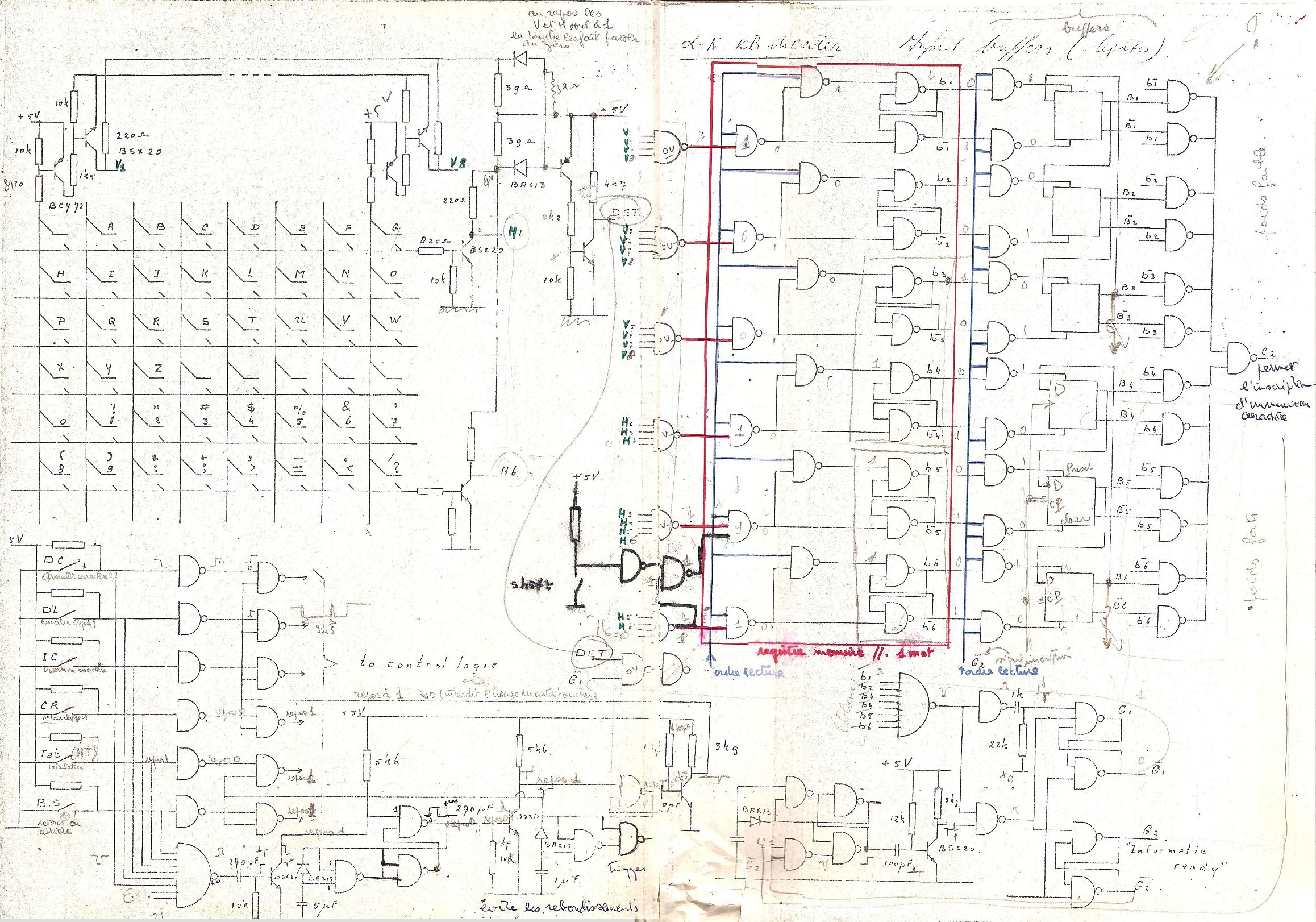
Keyboard study
The keyboard is made of 2
types of keys:
Touches de fonction
The anti-bounce circuit
The study of electrical contacts shows that there are many bounces (for a period of approximately 10 mS) Previously, we worked in electromechanical world, and the contact defects were not significant. The high speed electronics (1970) allowed to see all these bounces, which introduced numerous malfunctions. It was necessary to correct this by creating an anti-bouncing. This function is associated with each type of keys.
You can find a complete description of its operation here: AntiRebonds.pdf (Sorry in French. Notes of the time ... with faults!)
The ascii coding and register
ascii coding
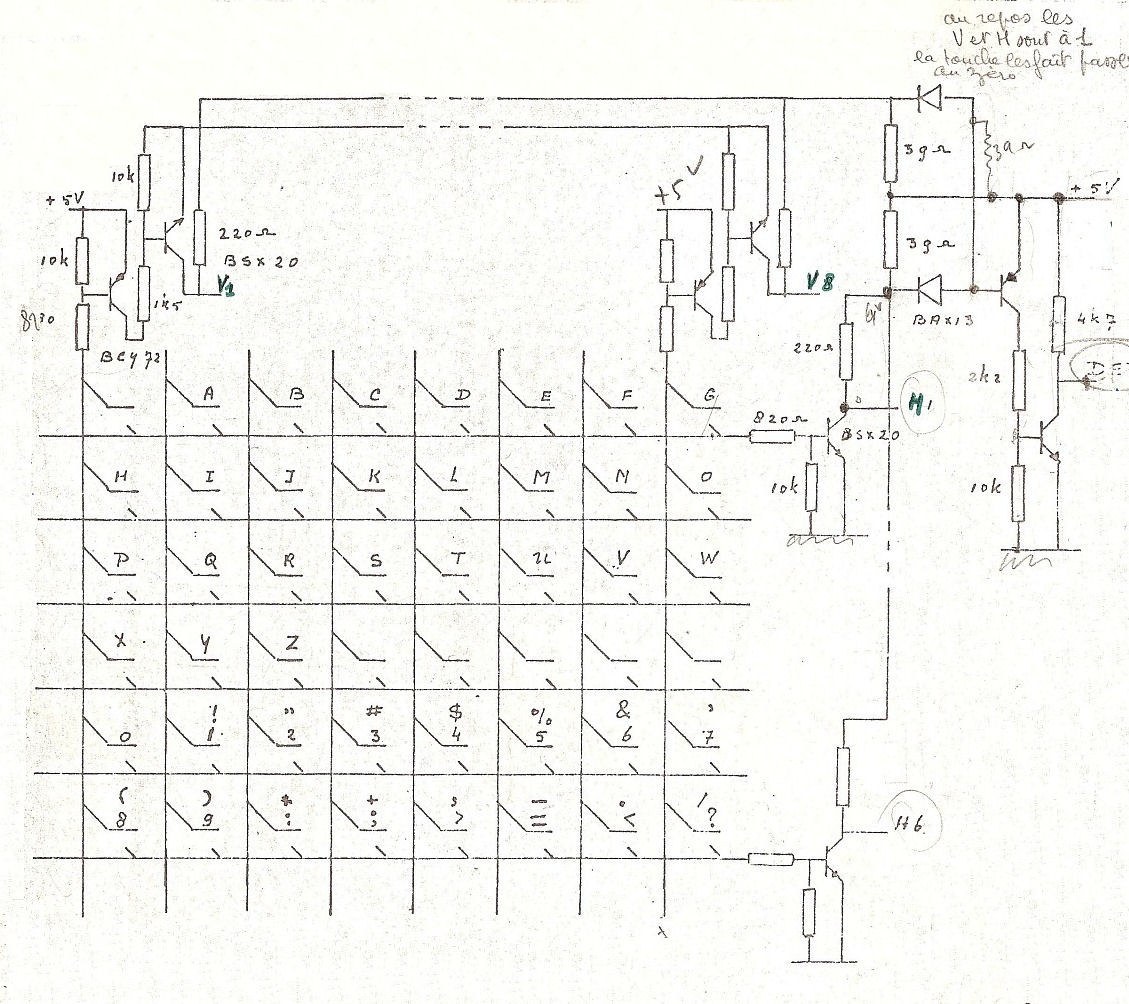
Complete layout and keyboard schematics
Schematics
- alphanumeric keys A..Z 0..9 and some signs like ! " # $ % & ' ( ) * + - =, . ; : ? / space which are arranged on a 6x8 matrix. A special shift key allows for the 64-character set.
Operation:
Contacts are
closing. Each column is associated to a pair of transistors
BCY72 and BSX20. The sensing element is the base of BCY72 linked to
the column with a 820 ohms. At rest, this 820 ohms is not connected,
leaving the base of the PNP fed by 5 volts: it is blocked.
Similarly, the horizontal lines are connected to the base of an NPN. At rest, the transistor is blocked.
A contact in a key, feeds a transistor column (bcy72) and a transistor line (bsx20).
The other transistors do not move!
So the logic should monitor the output levels of 8 pairs from the top (V1 to V8) and 6 transistors right (H1 to H6)
The circuit of the right, with the diodes, can detect the depress of a key (DET) and start the bouncing circuit.
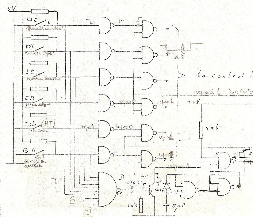
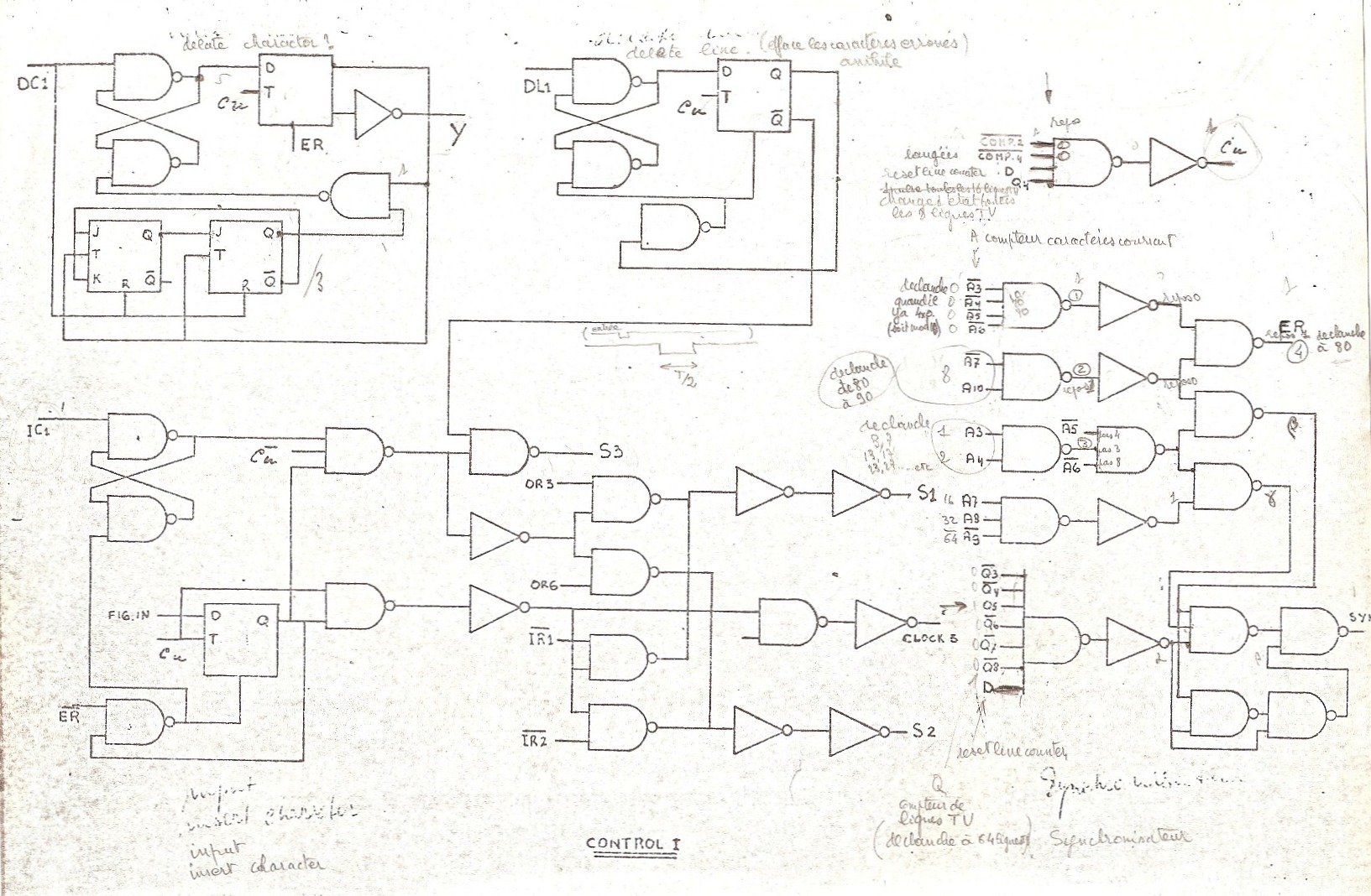
- Function keys were a new concept for the time: deletion, insertion of a character, deletion, insertion of a row of characters, returning to the line and back space. Remember, we knew only typewriters and teleprinters (Teletypes) Secretaries were putting white paint to delete a character!
Touches de fonction
The
circuit is not a matrix. Each key has its own circuit. The NAND8 acts
as OR
and detects if a key has been pressed. It enables
an anti-bouncing circuit.
(Which will be followed by a series of delays)
The anti-bounce circuit
The study of electrical contacts shows that there are many bounces (for a period of approximately 10 mS) Previously, we worked in electromechanical world, and the contact defects were not significant. The high speed electronics (1970) allowed to see all these bounces, which introduced numerous malfunctions. It was necessary to correct this by creating an anti-bouncing. This function is associated with each type of keys.
You can find a complete description of its operation here: AntiRebonds.pdf (Sorry in French. Notes of the time ... with faults!)
The ascii coding and register
ascii coding
Complete layout and keyboard schematics
Schematics
The tabs and some control circuits
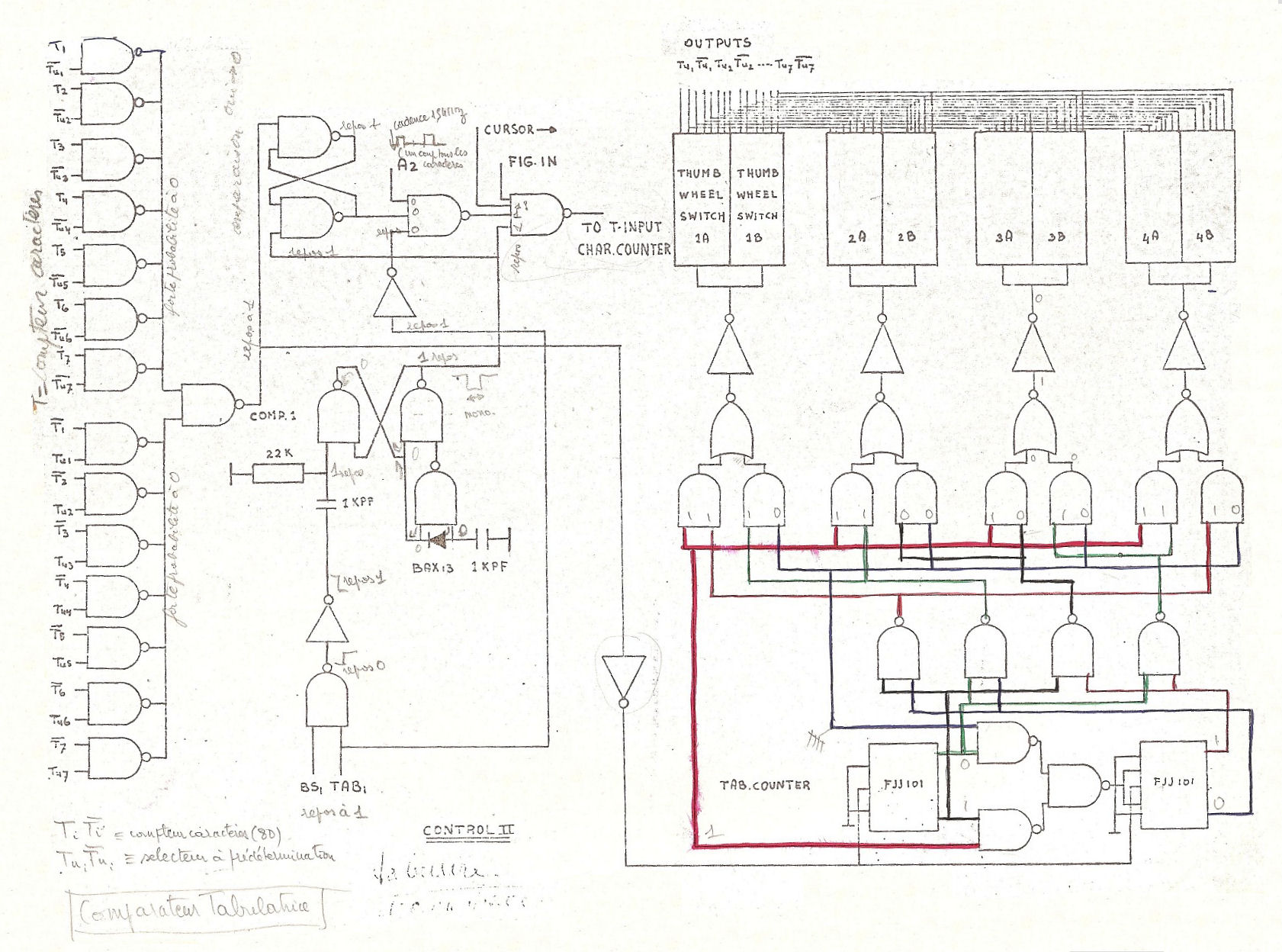
tabulation circuitry
We can see above,
left, a 2-bit counter to select one of 4 pairs of decimal encoder for
tabulation.
On the left a comparator with a system generating pulses until the correct position of the cursor is reached.
And below, the control signals for inserting / deleting characters or deleting rows of characters:
On the left a comparator with a system generating pulses until the correct position of the cursor is reached.
And below, the control signals for inserting / deleting characters or deleting rows of characters:
Logic controls, anti-bouncing...
Timings generation and cursor management
In
horizontal
Using a 13.9643 MHz crystal, we will get all frequencies useful in a visualization system. We saw the need to read 80 ascii codes within 52 uS (80: visible part of a line), which means that a full 64uS (visible + spot return) requires a count at 100 [52/80 x64 approx!]
These reasons why pre division by 3, then par3 (thus 9) will be followed by a divide-by-100 [10 followed by 10] to get 15516 Hz, which corresponds to the frequency scanning line with a television (in reality it should be 15 625 Hz)

A0..A10 running counter
Thus, a current meter (A0 to A10) will know the location of the spot on the screen:
Another counter up / down T1 .. T7 will determine the cursor position.

Cursor counter
To show the cursor on the screen, a logic establish the coincidence between the running counter A10 .. A3 and the cursor counter T7 .. T1

The comparator generates the symbol cursor
The full double page:

full schematics
Using a 13.9643 MHz crystal, we will get all frequencies useful in a visualization system. We saw the need to read 80 ascii codes within 52 uS (80: visible part of a line), which means that a full 64uS (visible + spot return) requires a count at 100 [52/80 x64 approx!]
These reasons why pre division by 3, then par3 (thus 9) will be followed by a divide-by-100 [10 followed by 10] to get 15516 Hz, which corresponds to the frequency scanning line with a television (in reality it should be 15 625 Hz)
A0..A10 running counter
Thus, a current meter (A0 to A10) will know the location of the spot on the screen:
- A2 .. A0 indicate the horizontal position of the spot in a character
- A10 .. A3 show for the first 80 states the position of a character in a row, and 20 following the horizontal return of the spot.
Another counter up / down T1 .. T7 will determine the cursor position.
- To the right -> down
- To the left -> up counting
Cursor counter
To show the cursor on the screen, a logic establish the coincidence between the running counter A10 .. A3 and the cursor counter T7 .. T1
The comparator generates the symbol cursor
The full double page:
full schematics
Vertically
We need a solution to determine the line in a character, and the selection of each of the 16 rows corresponding to the chip select delay lines.
We must also define the 54 lines needed for the return of field spot.
It must also be managing vertical cursor.
Since there is no compulsion regarding the delay in the chain of counting, we can take simple flip-flops. (15525)

Running vertical counter Q1..Q8
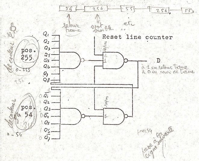
visible/invisible part 54/312

Vertical cursor counter for cursor generation
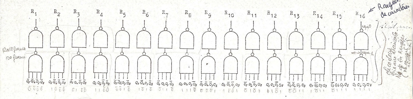
Delay Lines selects
(similar to 74'154)
The full double page:
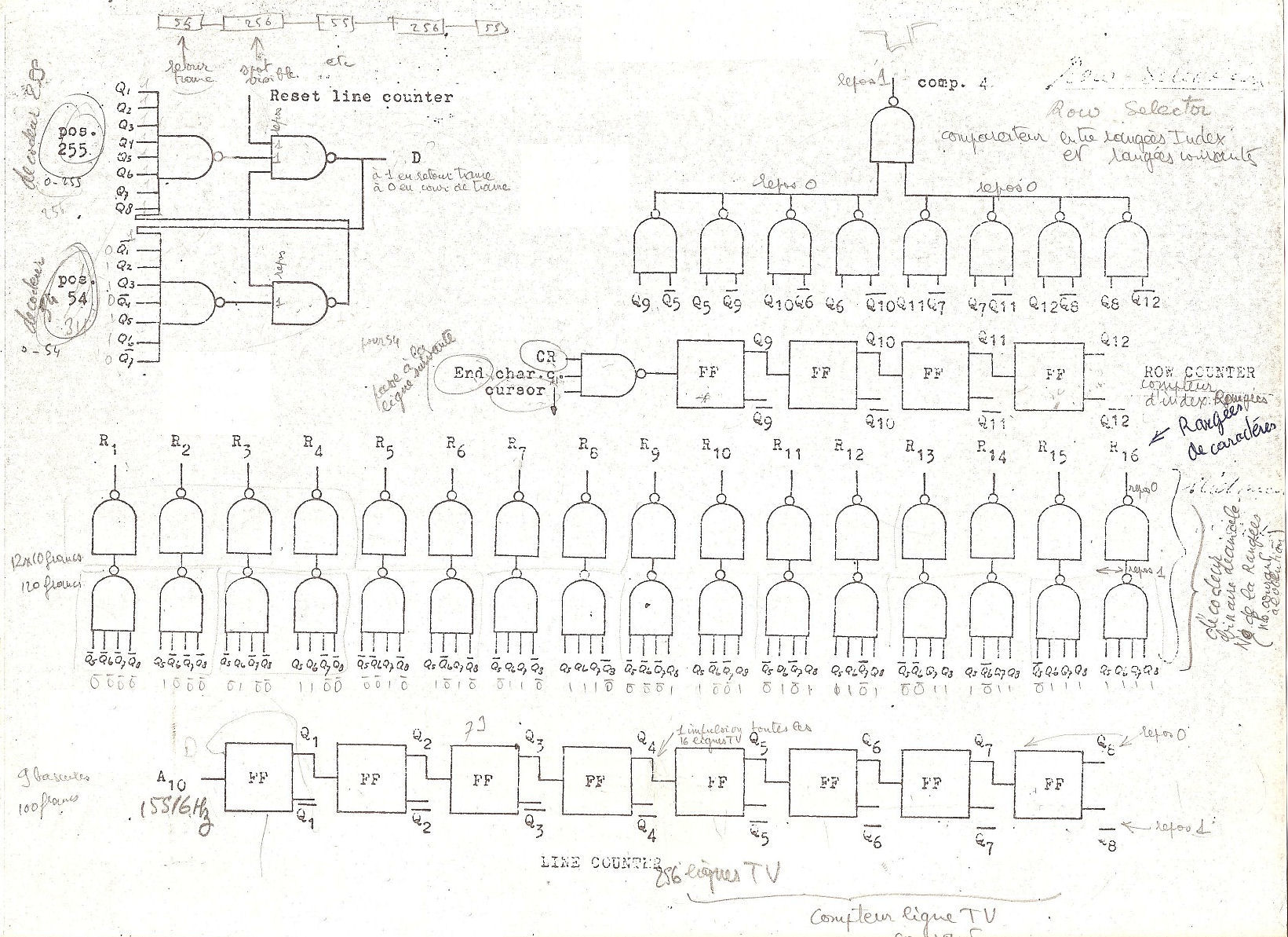
We need a solution to determine the line in a character, and the selection of each of the 16 rows corresponding to the chip select delay lines.
We must also define the 54 lines needed for the return of field spot.
It must also be managing vertical cursor.
Since there is no compulsion regarding the delay in the chain of counting, we can take simple flip-flops. (15525)
Running vertical counter Q1..Q8
visible/invisible part 54/312
Vertical cursor counter for cursor generation
Delay Lines selects
(similar to 74'154)
The full double page:
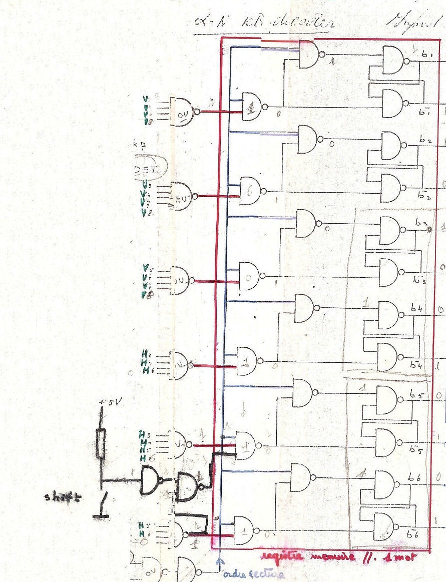
The delay line memory
We saw the need of 2 delay lines alternately, as a line could only remember that 300 bits. We are going to find a circuitry demultiplexing input and output multiplexing.
In output circuitry, we have 2 flip-flops for insertion / deletion of character functions. (It lengthens or shortens the length of shift)
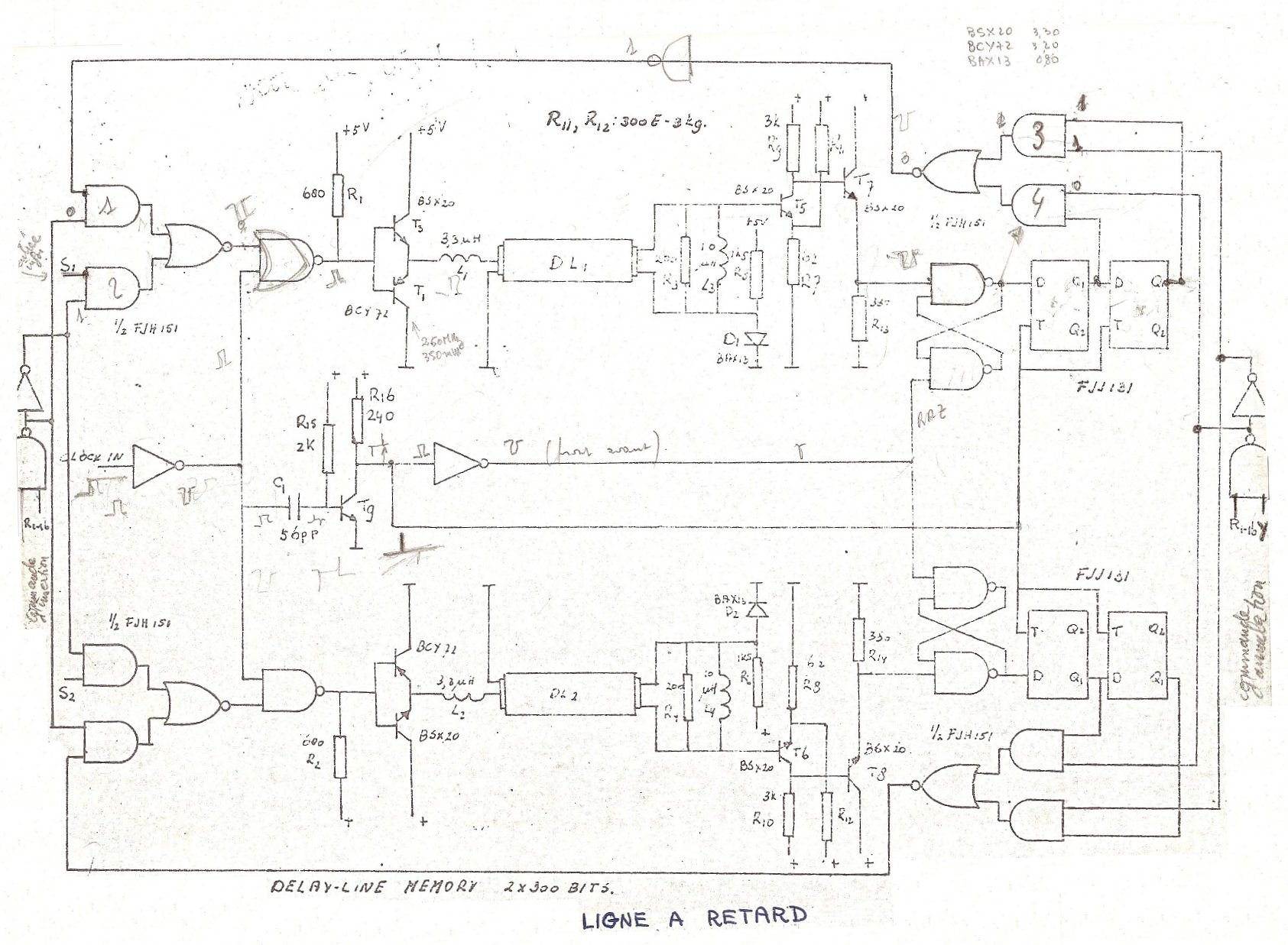
Writting and reading TV delay lines
Then, read the 32 delay lines and generate ascii code (short) which will be presented to 2 generators characters.
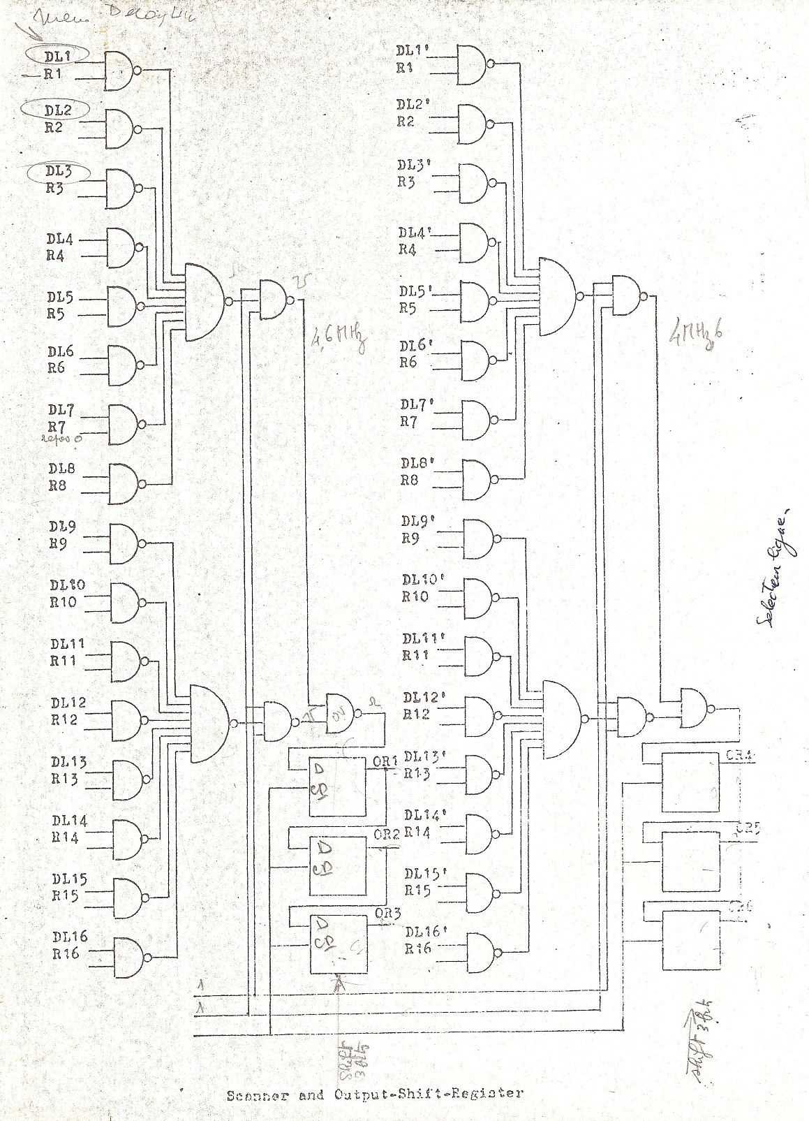
Output multiplexer
This is equivalent to 2x2 74'151 followed by a 74'174. The delay lines are mentally on the left.
Character generation
We must now get to the purpose of the machine: generate a video signal to be sent on a television monitor. It is therefore necessary to generate the graphics. This can be accomplished through specialized LSI circuit, FDR-116-Z1.
We must submit to this kind of circuit ascii code on 6 bits and the number of TV line
character to be displayed. (Q1 .. Q4 since there are 16 rows of characters in 256 visible lines)
Do not forget that for the sake of speed, it is necessary to have 2 CG in parallel ... The following will describe (in ascending order):
- A little glue logic to generate Phi1 phases 2 and Phi2 of N-MOS.
- A registry to store the ascii code
- A row of buffer TTL -> MOS
- 2 CG
- A row of buffers MOS -> TTL
- A row of 6x1 multiplexer bit
- Register / / classic series to be excited at the pace of pixels. (The highest frequency meter course)
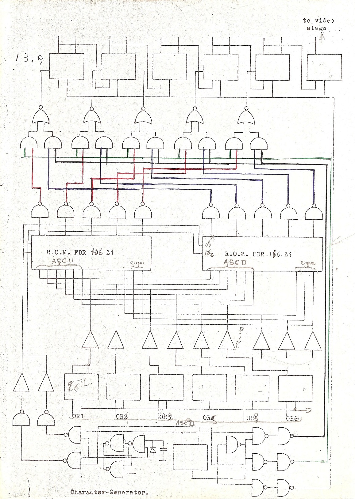
CG and shift register
Part list
This machine uses:


- 254 IC 14/16 pins DIL
- 186 transistors
- 50 diodes, 396 resistors, 32 TV Delay lines
- 40 capacitors
- 2 LSI MOS
- etc.
The evolution of this technics
In
about 1970 came the first integrated circuit memory. The industry began
with the use of shift registers, because we knew that
the shift registers provide greater integration than RAM
(random access). [The
same was made to shift counters to use fewer transistors ... Hence the
emergence of serial CPUs]
Shift registers were ideal for displaying data on screen, as they perfectly follow the movement of the TV spot. However writing information in the register was complicated and demanded complicated logics (should write on the fly). Remember that at the time microprocessors were not yet invented.
Look at the specification of any one of these new components: The FDN-106.pdf.
Such a component costs dearly anyway! I noted in 1970, a unit price of 240.00 francs! (1 / 15 of the salary of an engineer!) By optimizing (at the cost of a twisted, and therefore complicated design) a 10 chip memory costed for almost the salary of an engineer! For 1 kilo byte!
Conclusions
A big gas plant! (only
french joke?) Although easy to understand. It still points in the
shadow glues logics ... It really was looking in all directions to find
solutions to this lack of memory ... And was not afraid to explore new
paths. (Risky!)
Fortunately the first memory integrated circuits arrived quickly. The EPROM Intel 1702 to about 1972 (256 bytes). I do not remember as regards RAMs, but in 1974 there were 256 bits (see Beryllium board on this website)
The machines thus leaving factory built at a cost of 12000 francs (3 months salary engineer)
The trade could easily fight very poor reliability of teleprinters. (A breakdown per week)
In 1970, I wrote in a comparative study on the cost of memories:
"The cost per bit is about:
- 0.15 franc for the delay line
- 1.00 franc for dynamic shifts registers
- 2.40 francs for shifts static "
(In 1970: $1=about 5.00
francs. to be verified...)
The unit was the cost per bit!
The world market for this type of machine was estimated at 200 000 units (!)
Ah, in fact, it still lacks something important in this machine! Find yourself? "
The unit was the cost per bit!
The world market for this type of machine was estimated at 200 000 units (!)
Ah, in fact, it still lacks something important in this machine! Find yourself? "
Ended March 28, 2008 / translated on March 30 JMP